Charge-density wave (CDW) systems stand as the most prominent ones whose electronic properties strongly depend on the detailed atomic structures, which involve partial or full metal-insulator phase transitions. In these phase transitions the typical changes of bond length in the atomic structures are on the order of sub-angstrom, making the direct identification of atomic structures rather difficult for 2D CDW systems, where combined examinations of experiments and DFT-calculations could provide persuasive evidence about the atomic structures of them.
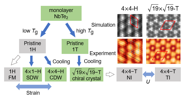
In a recent study, comparing first-principles-calculated orbital textures with reported STM measurement, Prof. Huang’s group successfully identify multiple CDWs in monolayer NbTe2. Surprisingly, they reveal that both 1T/1H phases could exist in monolayer NbTe2, which was incognizant before. Particularly, they find that the experimentally observed 4 × 4 and 4 × 1 CDWs could be attributed to 1H stacking while the observed ![]() phase could possess 1T stacking. The existence of 1T/1H phases results in competition between CDW, spin-density wave (SDW), and ferromagnetism in 1H stacking under external field and results in CDW-induced quantum phase transitions from Kramers-Weyl fermion to topological insulator in 1T stacking. Their study suggests NbTe2 as an exotic platform to investigate the interplay between CDW, SDW, and topological phases, which are largely unexplored in current experiments.
phase could possess 1T stacking. The existence of 1T/1H phases results in competition between CDW, spin-density wave (SDW), and ferromagnetism in 1H stacking under external field and results in CDW-induced quantum phase transitions from Kramers-Weyl fermion to topological insulator in 1T stacking. Their study suggests NbTe2 as an exotic platform to investigate the interplay between CDW, SDW, and topological phases, which are largely unexplored in current experiments.
This study has been published in Nano Letters in 2024.

Figure 1. Identification of multiple CDW states and their properties in monolayer NbTe2. Tg: growth temperature; FM: ferromagnetism; SDW: spin-density wave; CDW: charge-density wave; NI: normal insulator; TI: topological insulator.
[1] H. Jin, W. Tan, and B. Huang, Nano Lett., doi.org/10.1021/acs.nanolett.4c02621 (2024).


